

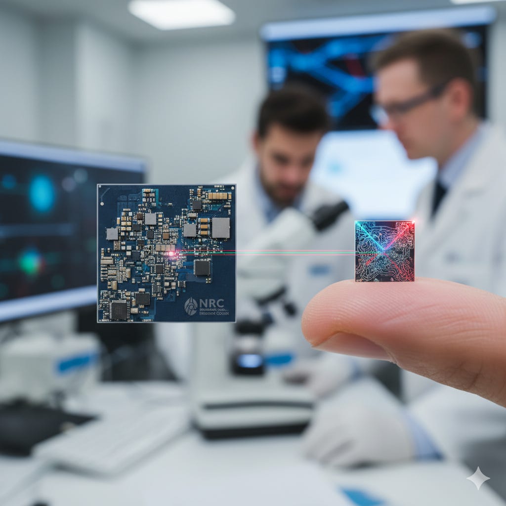
NRC-Backed Research Slashes Chip Size by 90%
A new design method from Canadian researchers dramatically shrinks optical components, paving the way for faster, more powerful data processing in a hyper-connected world.

Connecting to the massive surge in global data consumption from cloud computing, AI, and video streaming, you’ve likely felt the digital world getting faster. But behind the scenes, the physical hardware is straining against fundamental limits. The electronic components that power our digital infrastructure are hitting a performance bottleneck, and even their light-based successors—photonic circuits—are limited by how small they can be made. A recent research paper, co-authored by scientists at Canada’s National Research Council (NRC), details a breakthrough that directly tackles this physical barrier, offering a path to dramatically smaller and more efficient optical devices.
The Miniaturization Problem
Why Size Matters in Photonics
To meet the insatiable demand for data, engineers turned to silicon photonics, a technology that uses light instead of electrons to transmit information. As the research paper explains, this approach offers massive bandwidth and is compatible with existing chip manufacturing processes. However, unlike transistors that have shrunk exponentially for decades, the miniaturization of photonic devices is inherently limited by the physics of light diffraction.
Key components like optical switches, which route signals, have stubbornly large footprints. The study notes that conventional designs, such as Mach-Zehnder interferometers (MZIs), can occupy thousands of square micrometers. This physical size is a major obstacle to increasing bandwidth density and scaling up the capacity of optical interconnects needed for next-generation computing, phased arrays, and even quantum information processing.
A New Design Philosophy
Thinking with Temperature
The researchers, including two from the NRC, pioneered a novel approach called thermo-optic-enabled topological optimization. Instead of relying on conventional, physics-based design rules, this method uses a powerful computer algorithm to invent a new device structure from the ground up.
Here’s the key innovation: the algorithm simultaneously considers how the device should perform at two different temperatures. It leverages the thermo-optic effect, where the refractive index of silicon—the material that guides the light—changes subtly with temperature. By treating temperature as a core design parameter, the optimizer can generate a non-intuitive, complex structure that performs one function at room temperature and a completely different one when heated.
The design process starts with a blank slate—a tiny rectangular area—and iteratively adjusts the material properties of thousands of individual pixels, deciding whether each tiny point should be silicon or silica. The goal, or ‘figure of merit,’ is to guide a light signal to one output port at 300 K (room temperature) and to a second output port when the device is heated to 405 K.
The Breakthrough Device
A Switch and Splitter in One
The result of this new methodology is an ultra-compact optical switch with a footprint of just 10 µm by 6 µm. The research paper highlights that this is a drastic reduction, making it about a tenth of the size of conventionally designed switches while delivering comparable performance in insertion loss and signal quality.
The algorithm’s final design is remarkable. It works by strategically placing minuscule silica features, which make up less than 5% of the total design area, to act as light scatterers. These features create a precise interference pattern that directs light to the correct output based on the temperature-induced change in silicon’s refractive index.
Remarkably, the device also functions as a tunable power splitter—a capability that emerged naturally from the design without being explicitly programmed into the optimization. At intermediate temperatures, the device can split an incoming optical signal into any desired ratio, from 100:0 to 0:100. This dual functionality is achieved within a footprint that is 90% smaller than conventional splitters.
After simulating the design, the team fabricated and tested a physical prototype. The experimental results closely matched the simulations, confirming the success of the temperature-aware optimization process. The device demonstrated the ability to correct for small fabrication errors simply by tuning the on-chip heater, showcasing a robustness critical for real-world applications.
The Data Brief
The Problem: The physical size of silicon photonic components is limiting the growth of data processing capacity. Conventional optical switches are too large for the density required in modern data centers.
The Innovation: Researchers, including scientists from the National Research Council of Canada, developed a new “temperature-aware” topological optimization method that designs optical devices by treating temperature as a core functional parameter.
The Result: An experimentally validated optical switch that is 90% smaller than conventional designs (60 µm²) but offers comparable performance.
Dual Functionality: The same ultra-compact device also operates as a fully tunable optical power splitter, a valuable secondary function that emerged from the novel design process.
The Implication: This work unlocks a new path toward densely integrated photonic circuits, enabling more powerful and efficient optical interconnects for data centers, AI hardware, and quantum computing.
A Foundational Shift in Photonic Design
This research represents more than just an incremental improvement; it signifies a foundational shift in how we approach the design of complex photonic devices. By entrusting an optimization algorithm with the creative process and expanding its toolkit to include thermodynamics, the researchers have unlocked a level of compactness and functionality that was previously unattainable through conventional, human-driven methods. This NRC-backed work is a powerful demonstration of how public investment in fundamental science can produce the intellectual frameworks necessary to solve the critical engineering challenges of tomorrow. Innovation isn’t just about making things better; it’s about finding entirely new ways to begin.
Source Documents
Rogers, R., Xu, D.-X., Grinberg, Y., & Liboiron-Ladouceur, O. (2025). Thermo-optic-enabled topological optimization for tunable ultra-compact silicon photonic device design. Optics Express, 33(17), 35536–35549.